Choosing the right snus packaging machinery in Togo requires a practical mix of technical knowledge, awareness of local customs and regulations, and an understanding of
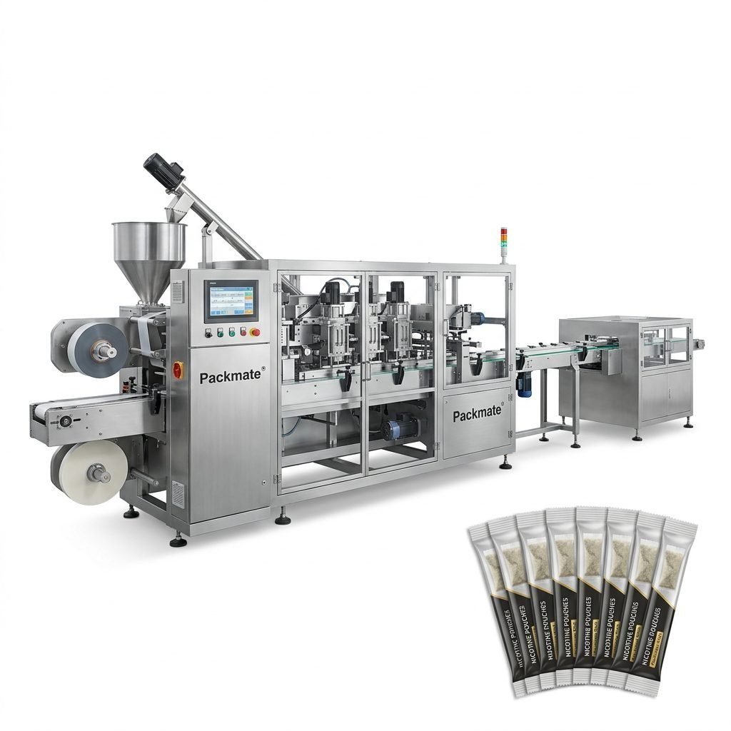
Choosing the right snus packaging machine in Burundi involves more than just matching a machine to a product. It requires understanding local market habits, regulatory
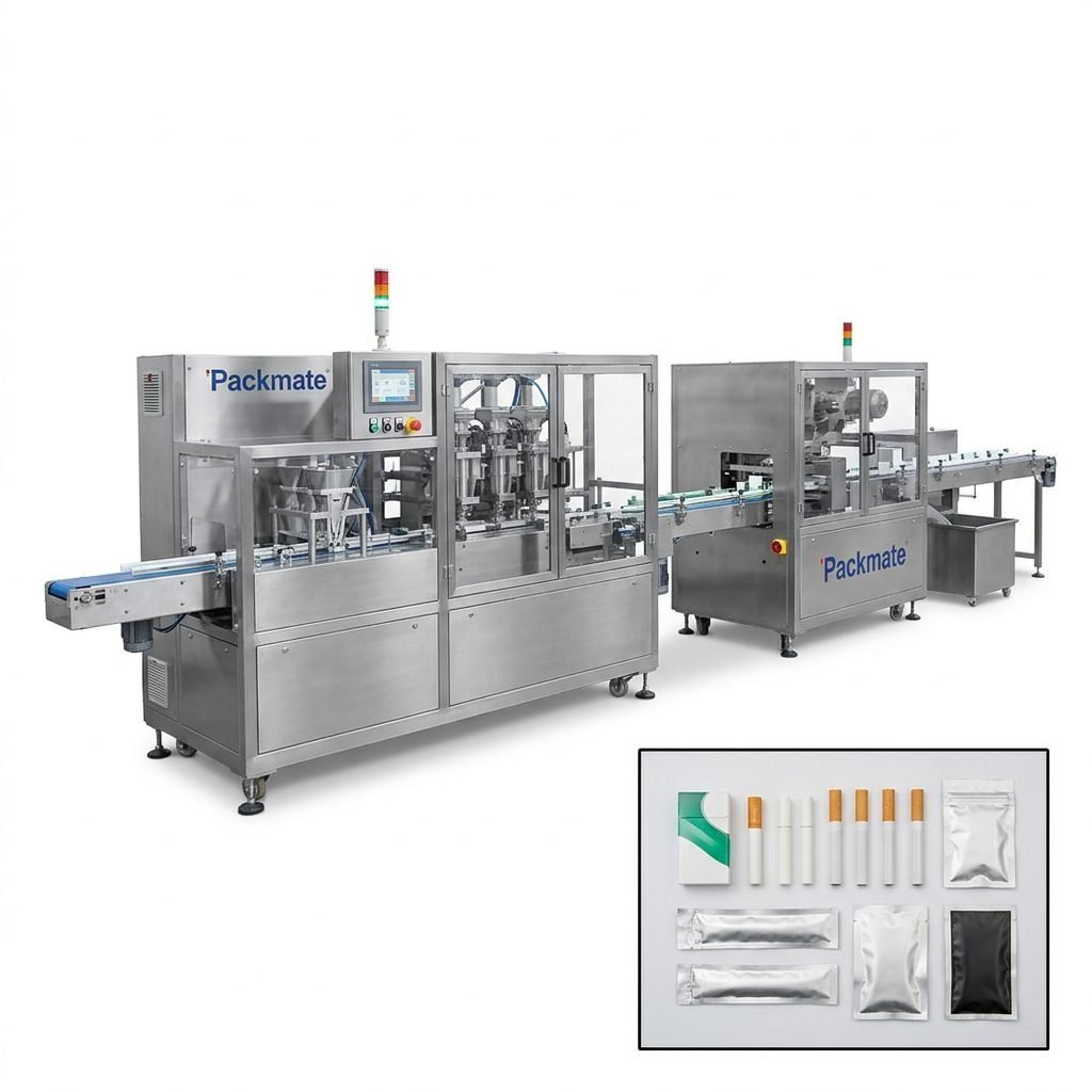
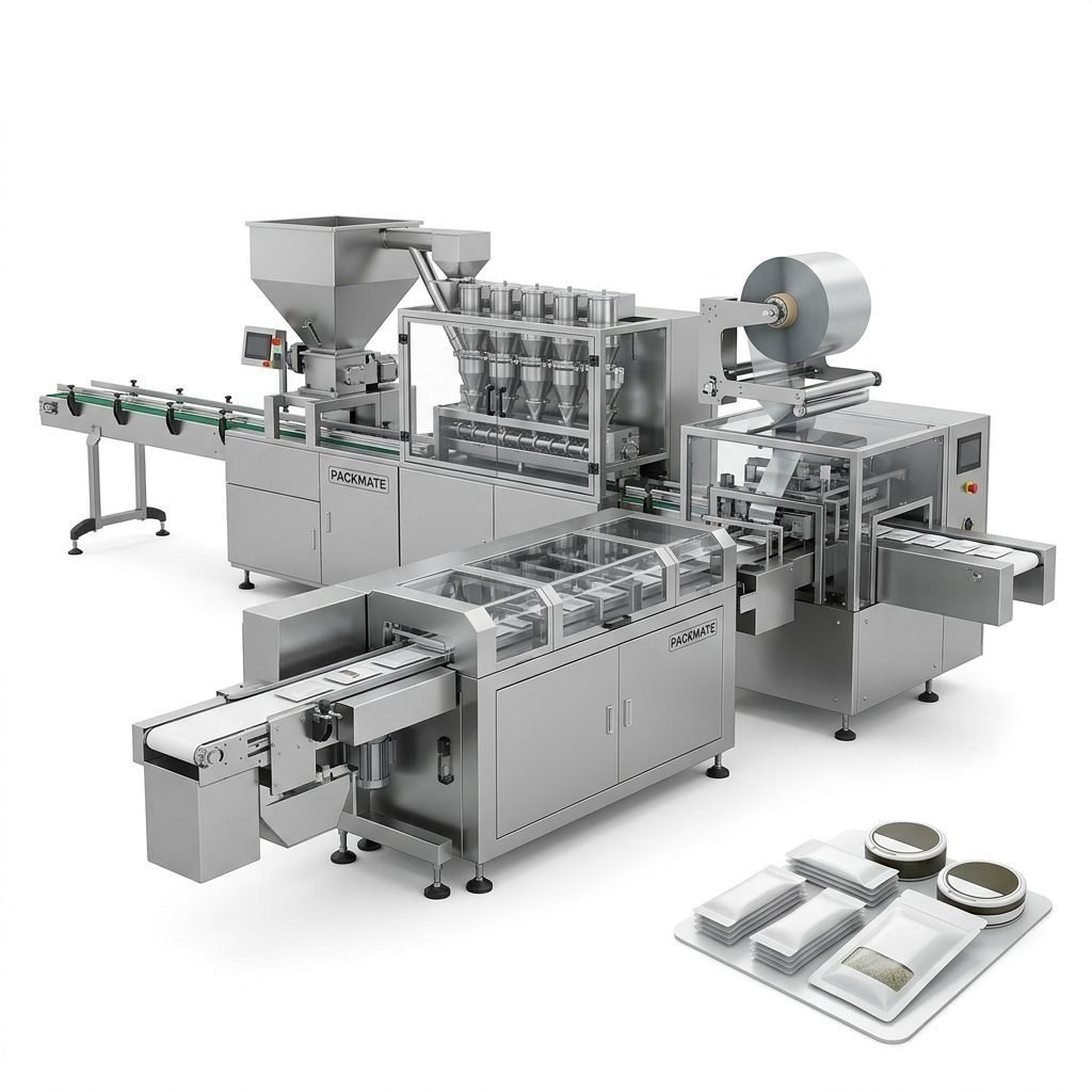
Choosing the right snus packaging machine supplier for your factory in Norway is a strategic decision that affects production efficiency, compliance, and long-term profitability. This